Circuit boards have developed from single-sided to double-sided, multi-layer, and rigid-flex board, and still maintain their respective development trends. Due to the continuous development of high precision, high density and high reliability, continuous reduction in size, cost reduction, and performance improvement, printed circuit boards will still maintain strong vitality in the future development of electronic equipment. So, what are the steps of circuit board design?
PCB design
1. Preliminary preparation
Including the preparation of component libraries and schematic diagrams. Before proceeding with PCB design, we must first prepare the schematic SCH component library and PCB component packaging library. The pcb assembly manufacturer component package library is best established by the engineer based on the standard size data of the selected device. PCB component packaging library requirements are high, it directly affects the installation of PCB, schematic diagram SCH component library requirements are relatively loose, but pay attention to define the pin attributes and the corresponding relationship with the PCB component packaging library.
2. PCB structure design
According to the determined circuit board size and various mechanical positioning, draw the PCB frame in the PCB design environment, and place the required connectors, buttons/switches, screw holes, assembly holes, etc. according to the positioning requirements.
3. PCB layout design
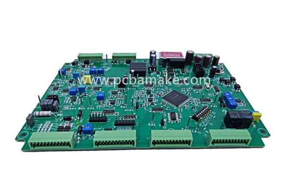
The layout design is to place the components in the PCB frame according to the design requirements. Generate the net list in the schematic tool, and then import the net list in the PCB software. After the netlist is successfully imported, it will exist in the background of the software. Through the Placement operation, all devices can be called out, and there is a flying line prompt connection between the pins. At this time, the layout design of the device can be carried out. PCB layout design is the first important process in the entire PCB design process. The more complex the PCB board, the better the layout can directly affect the difficulty of later wiring.
4. PCB wiring design
PCB layout design is the process with the largest workload in the entire PCB design, which directly affects the performance of the PCB board. In the PCB design process, there are generally three realms of wiring. The first is the layout, which is the most basic entry requirement for PCB design; the second is the satisfaction of electrical performance, which is the standard to measure whether a PCB is qualified. After the wiring is laid out, carefully adjust the wiring to achieve the best The electrical performance; again, neat and beautiful, messy wiring, even if the electrical performance is passed, it will bring great inconvenience to the later modification of the board and test and repair. The wiring requirements are neat and uniform, and it cannot be crisscrossed and disordered.
5. Wiring optimization and silk screen placement
"PCB design is not the best, only better", "PCB design is an art of defects", this is mainly because PCB design needs to realize the design requirements of all aspects of hardware, and individual requirements may be in conflict with each other. Bear's paw can't have both.
6. Network DRC inspection and structure inspection
Quality control is an important part of the PCB design process. General quality control methods include: design self-inspection, design mutual inspection, expert review meetings, special inspections, etc. Schematic diagram and structural element diagram are the most basic design requirements. Network DRC inspection and structural inspection are to confirm that the PCB design meets the two input conditions of the schematic netlist and structural element diagram.
7. PCB plate making
Before the PCB is officially processed and manufactured, the circuit board designer needs to communicate with the PCB supplier's EQ to answer the manufacturer's confirmation questions about the PCB board processing. This includes, but is not limited to, the selection of PCB board model, the adjustment of circuit layer line width and line spacing, the adjustment of impedance control, the adjustment of PCB multilayer circuit board stacking thickness, surface treatment processing technology, aperture tolerance control and delivery standards, etc.